
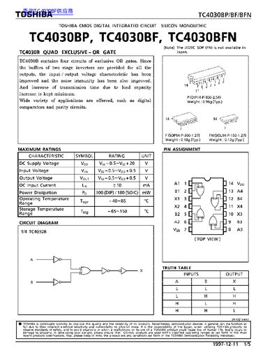
TOSHIBA TC4030BP TC4030BF TC4030BFN handbook


TOSHIBA TC4030BP TC4030BF TC4030BFN handbook - cover page
Brand
Toshiba
Category
Chips
Document type
Datasheet
Language
English
Pages
5
File format
PDF
File size
203 KB
Published
07 June, 2012
Updated
07 June, 2012
MD5 checksum
084AB49EE8545023B585C79DA6D4C5F9

About this manual

This document is a technical datasheet for the Toshiba TC4030BP, TC4030BF, and TC4030BFN integrated circuits. The device contains four exclusive OR gates with two-stage inverter buffers to improve input/output voltage characteristics and noise immunity. It supports wide applications including comparators and parity circuits.

What's inside

  • Maximum Ratings
  • Pin Assignment
  • Circuit Diagram
  • Truth Table
  • Recommended Operating Conditions
  • Static Electrical Characteristics
  • Dynamic Electrical Characteristics
  • Package Outlines

Specifications

Number of GatesFour circuits of exclusive OR gates
DC Supply Voltage (Max)+20 V
Operating Temperature Range-40 to +85 C
Storage Temperature Range-65 to +150 C
Power Dissipation (DIP)300 mW

Frequently asked questions

What is the typical weight of a DIP package?

The typical weight for a DIP package is 0.96g.

Download PDF (203 KB)

More Toshiba Manuals


View all Toshiba manuals →