
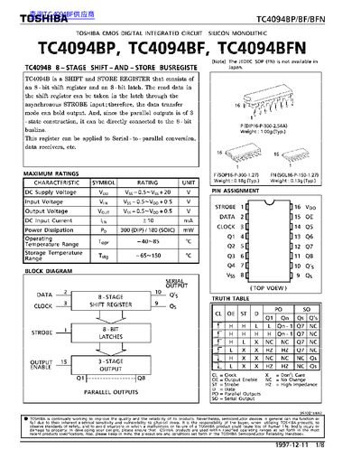
This document is a technical datasheet for the Toshiba TC4094BP, TC4094BF, and TC4094BFN integrated circuits. The device functions as an 8-bit shift register combined with an 8-bit latch, designed to facilitate serial-to-parallel conversion and data reception applications.
The document provides comprehensive electrical specifications including maximum ratings, static and dynamic characteristics, and timing diagrams. It covers three package types: DIP16, SOP16 (200mil body), and SOL16 (150mil body), noting that the FN package is not available in Japan.
| Number of Stages | 8-stage |
|---|---|
| Supply Voltage Range | 3 to 18 V |
| Operating Temperature Range | -40~+85 °C |
| Max Clock Frequency (Vcc=3V) | 2.5 MHz |
| Min Clock Pulse Width (Vcc=3V) | 20 ns |
It is an 8-bit shift register and an 8-bit latch used for serial-to-parallel conversion.
No, the JEDEC SOP (FN) package is not available in Japan.