
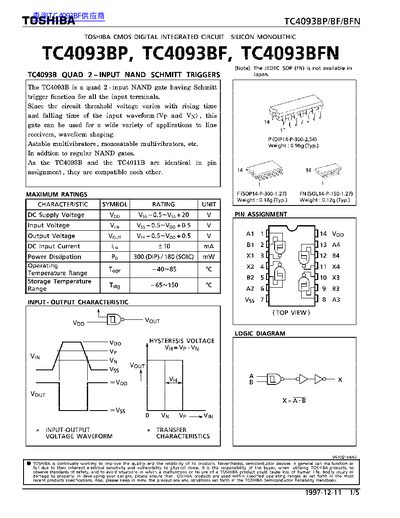
TOSHIBA TC4093BP TC4093BF TC4093BFN handbook


TOSHIBA TC4093BP TC4093BF TC4093BFN handbook - cover page
Brand
Toshiba
Category
Chips
Document type
Datasheet
Language
English
Pages
5
File format
PDF
File size
213 KB
Published
07 June, 2012
Updated
07 June, 2012
MD5 checksum
1ECB67E013824012730CA48BA0D6C858

About this manual

This document is a technical datasheet for the Toshiba TC4093B series of CMOS digital integrated circuits. The device features a quad 2-input NAND gate configuration where all input terminals possess Schmitt trigger functionality, allowing it to be used for waveform shaping and line receivers due to its variable threshold voltage based on rising and falling times.

What's inside

  • Description
  • Maximum Ratings
  • Recommended Operating Conditions
  • Static Electrical Characteristics
  • Dynamic Electrical Characteristics
  • Package Outline Drawings

Specifications

Operating Temperature Range-40 to +85 °C
Storage Temperature Range-65 to +150 °C
Power Dissipation (DIP)300 mW

Frequently asked questions

What are the maximum DC supply voltage ratings for this circuit?

The device can operate with a DC supply voltage between -0.5V and +20V.

What is the typical weight of the DIP14 package?

The typical weight for the DIP14 package is 0.96g.

Download PDF (213 KB)

More Toshiba Manuals


View all Toshiba manuals →