
TOSHIBA TC4049BP/BF/BFN TC4050BP/BF/BFN handbook


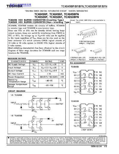
TOSHIBA TC4049BP/BF/BFN TC4050BP/BF/BFN handbook - cover page
Brand
Toshiba
Category
INTEGRATED CIRCUITS
Document type
Datasheet
Language
English
Pages
5
File format
PDF
File size
231 KB
Published
07 June, 2012
Updated
07 June, 2012
MD5 checksum
0242CF1966B725769FB321B8E218AC6C

About this manual

This document provides technical specifications for the Toshiba TC4049BP/BF/BFN (inverting type) and TC4050BP/BF/BFN (non-inverting type) CMOS digital integrated circuits. These devices contain six buffer circuits designed to interface between CMOS logic levels and TTL or DTL systems, capable of driving large output currents.

What's inside

  • Maximum Ratings
  • Recommended Operating Conditions
  • Static Electrical Characteristics
  • Dynamic Electrical Characteristics
  • Pin Assignment
  • Circuit Diagram
  • Package Outlines

Specifications

Power Dissipation (DIP)300 mW
Number of CircuitsSix circuits of buffers

Frequently asked questions

What is the maximum DC supply voltage for these circuits?

The maximum DC supply voltage rating is +18 volts.

How much power does a DIP package dissipate at most?

A DIP package can dissipate up to 300 milliwatts.

What is the typical weight of a TC4050BFN package?

The typical weight for this package is 0.13 grams.

Download PDF (231 KB)

More Toshiba Manuals


View all Toshiba manuals →