
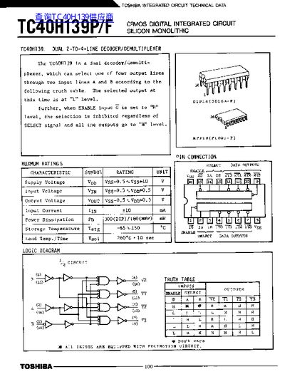
This document provides technical data for the TC40H139, a CMOS digital integrated circuit designed as a dual decoder/demultiplexer. The device allows selection of one of four output lines through two input lines (A and B) based on specific logic levels.
The datasheet details recommended operating conditions, including supply voltage ranges from 2.0V to 8.0V and an operating temperature range of -49°C to +85°C. It also lists electrical characteristics such as output voltages, input currents, power dissipation, and switching times for propagation delays.
| Supply Voltage (VDD) | 2.0 - 8.0 V |
|---|---|
| Operating Temperature (Topr) | -49 - 85 °C |
| Power Dissipation (DIP) | 300 mW |
| Input Capacitance (Cin) | 5 pF |
The device operates with a maximum supply voltage of 8.0 V.
A DIP package dissipates up to 300 mW of power.
The unit can operate between -49 and 85 degrees Celsius.