
IRF1310NS/L HEXFET® is an extremely efficient and reliable power device from International Rectifier company, which utilizes advanced processing techniques to achieve extremely low on-resistance per silicon area. This benefit, combined with the fast switching speed and ruggedized device design that HEXFET Power MOSFETs are well known for, provides the designer with an extremely efficient and reliable device for use in a wide variety of applications. The D2Pak is a surface mount power package capable of accommodating die sizes up to HEX-4. It provides the highest power capability and the lowest possible on- resistance in any existing surface mount package. The D2Pak is suitable for high current applications because of its low internal connection resistance and can dissipate up to 2.0W in a typical surface mount application. The through-hole version (IRF1310NL) is available for low- profile applications.
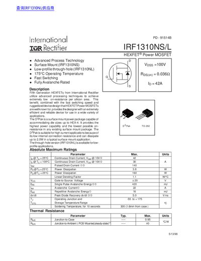
The IRF1310NS/L is a HEXFET® Power MOSFET offering low on‑resistance, fast switching, and avalanche capability for high‑efficiency power designs. It is available in a surface‑mount D?Pak package (IRF1310NS) and a low‑profile through‑hole version (IRF1310NL).
The document lists absolute maximum ratings, electrical characteristics, thermal parameters, and mechanical dimensions, along with recommended soldering conditions and tape‑and‑reel handling information. It also provides typical performance curves and test circuit diagrams for designers.
| Pulsed Drain Current (I_DM) | 140 A |
|---|---|
| Power Dissipation @ 25°C (P_D) | 3.8 W |
| Gate‑to‑Source Voltage (V_GS) | +20 V |
| Single Pulse Avalanche Energy (E_AS) | 420 mJ |
| Junction‑to‑Case Thermal Resistance (R_JC) | 0.95 °C/W |
| Operating Temperature Range | -55 °C to +175 °C |
A soldering temperature of 300 °C for 10 seconds is recommended.
The device is rated for a gate‑to‑source voltage of up to +20 V.