
The RQ1E070RP is an N-channel power MOSFET with a maximum rated voltage of -30V and a maximum continuous drain current of -7A. It features low on-resistance, built-in G-S protection diode, small surface mount package (TSMT8) and lead-free lead plating, RoHS compliant.
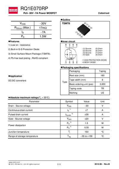
The RQ1E070RP is a -30 V, -7 A power MOSFET offered in a small TSMT8 surface‑mount package. The datasheet provides absolute maximum ratings, detailed electrical parameters, thermal data and mechanical dimensions for designers.
Key specifications include a drain‑source voltage of –30 V, continuous drain current of –7 A, pulsed current up to 28 A, gate‑source voltage of +20 V, and a junction‑to‑ambient thermal resistance of 83.3 °C/W. Package dimensions, pin layout and typical application curves are also included.
| Drain‑Source voltage (V_DSS) | -30 V |
|---|---|
| Continuous drain current (I_D) | -7 A |
| Pulsed drain current (I_D,pulse) | +28 A |
| Gate‑Source voltage (V_GS) | +20 V |
| Power dissipation (P_D) | 7 W |
| Junction temperature (Tj) | 150 °C |
| Storage temperature range | -55 °C to +150 °C |
| Thermal resistance, junction‑ambient (RθJA, typ.) | 83.3 °C/W |
| Input capacitance (Ciss) | 2700 pF |
| Output capacitance (Coss) | 390 pF |
| Reverse transfer capacitance (Crss) | 350 pF |
| Turn‑on delay time (t_on) | 16 ns |
| Rise time | 35 ns |
| Turn‑off delay time (t_off) | 140 ns |
| Fall time | 70 ns |
The device is rated for a maximum drain‑source voltage of –30 V.
It can conduct a continuous drain current of –7 A.
The MOSFET is supplied in a TSMT8 surface‑mount package.
Typical junction‑to‑ambient thermal resistance is 83.3 °C/W.