
This document describes the features and characteristics of the RYC002N05 Nch MOSFET produced by ROHM, including high-speed switching, small package size, and ultra-low voltage drive.
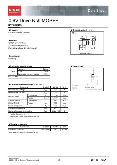
The RYC002N05 is a low‑voltage, high‑speed N‑channel MOSFET offered in a SOT‑23 package. The document provides detailed electrical characteristics, absolute maximum ratings, and typical performance curves for designers.
Key sections include features, packaging, maximum ratings, thermal resistance, electrical characteristics, body‑diode data, measurement circuits, and legal notices. All specifications are presented with typical conditions and limits for reliable circuit design.
| Drain‑source voltage (VDS) | 50 V |
|---|---|
| Gate‑source voltage (VGS) | +8 V |
| Continuous drain current (ID) | 200 mA |
| Pulsed drain current (ID,pulse) | 800 mA |
| Source current (IS) | 150 mA |
| Power dissipation (PD) | 200 mW |
| Maximum channel temperature (TCH) | 150 °C |
| Storage temperature range | -55 °C to +150 °C |
| Thermal resistance (RθJA) | 625 °C/W |
| Input capacitance (Ciss) | 26 pF |
| Output capacitance (Coss) | 6 pF |
| Reverse transfer capacitance (Cres) | 3 pF |
| Turn‑on delay time (t_on) | 5 ns |
| Rise time (t_rise) | 8 ns |
| Turn‑off delay time (t_off) | 17 ns |
| Fall time (t_fall) | 43 ns |
| Forward voltage of body diode (VF) | 1.2 V |
The device can withstand up to 50 V between drain and source.
The gate‑threshold voltage (VGS(th)) ranges from 0.3 V to 0.8 V.
The datasheet specifies a maximum power dissipation of 200 mW.