
2SK1151(L)(S), 2SK1152(L)(S) are N-channel MOSFETs that are suitable for high-speed power switching. Features include low on-resistance, high switching speed, low drive current, no secondary breakdown, and are suitable for switching regulators and DC-DC converters.
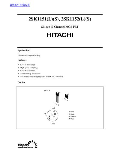
The document provides the electrical characteristics, absolute maximum ratings, and typical performance curves for the Hitachi 2SK1151(L)(S) and 2SK1152(L)(S) silicon N‑channel MOSFETs. It includes application notes for high‑speed power switching, features such as low on‑resistance and no secondary breakdown, and cautions for proper use.
Key sections cover absolute maximum ratings, detailed electrical parameters, temperature derating, transfer characteristics, and body‑diode behavior. The final pages contain legal notices and contact information for Hitachi Semiconductor worldwide.
| Drain‑to‑source voltage (Vds) | 450 V (2SK1151) / 500 V (2SK1152) |
|---|---|
| Gate‑to‑source voltage (Vgs) | +30 V |
| Drain current (Id) | 1.5 A |
| Power dissipation (Pch) | 20 W |
| Storage temperature range | -55 °C to +150 °C |
| Body‑to‑drain diode forward voltage | 1.0 V at 1.5 A |
The 2SK1151 is rated for a maximum drain‑to‑source voltage of 450 V.
The device should be used with a duty cycle of less than 1 % for pulse widths under 10 µs.
The MOSFET can be stored between –55 °C and +150 °C.
Yes, it has a body‑to‑drain diode with a forward voltage of about 1.0 V at 1.5 A.