
2SK1088-M is a N-channel MOS-FET manufactured by FUJITSU. Its features are high current, low on-resistance, no secondary breakdown, low driving power and high forward transconductance. This device is suitable for motor control, general purpose power amplifier and DC-DC converters applications.
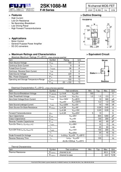
The 2SK1088-M is a high‑current, low‑on‑resistance N‑channel MOSFET from FUJI ELECTRIC's F‑III series. It is suited for motor control, power amplifiers and DC‑DC converters. The document lists maximum ratings, electrical parameters, thermal data and typical performance curves.
Key specifications include a 150 V drain‑source voltage, 9 A continuous drain current, 0.20 Ω typical on‑state resistance at VGS = 10 V, and a maximum power dissipation of 35 W. Thermal resistance is 62.5 °C/W (junction‑to‑air) with detailed capacitance and switching time figures.
| Drain‑Source Voltage (VDS) | 150 V |
|---|---|
| Continuous Drain Current (ID) | 9 A |
| On‑State Resistance (RDS(on)) typical at VGS=10 V | 0.20 Ω |
| Gate Threshold Voltage (VGS(th)) typical | 1.5 V |
| Maximum Power Dissipation (PD) | 35 W |
| Thermal Resistance (junction‑to‑air) Rth(ch‑a) | 62.5 °C/W |
| Input Capacitance (Ciss) | 900 pF |
| Turn‑On Time (t_on) | 10‑15 ns |
The device can withstand up to 150 V between drain and source.
The typical RDS(on) is 0.20 Ω when VGS is 10 V.
The MOSFET can dissipate up to 35 W under the specified conditions.
The junction‑to‑air thermal resistance is 62.5 °C/W.