
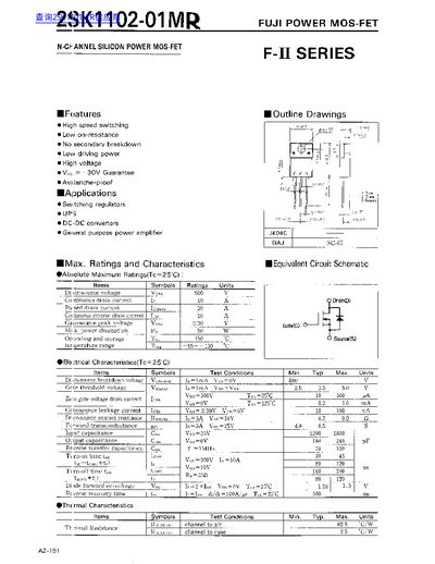
FUJI 2SK1102-01MP handbook


FUJI 2SK1102-01MP handbook - cover page
Brand
FUJI
Category
Other Electronics
Document type
Datasheet
Language
English
Pages
4
File format
PDF
File size
170 KB
Published
01 June, 2012
Updated
28 June, 2012
MD5 checksum
1EED7589505CDE06DBF342EBB8E65EEA

About this manual

The FUJI 2SK1102-01MR is a high‑speed, low‑on‑resistance power MOS‑FET designed for switching regulators, UPS, DC‑DC converters, and general‑purpose power amplification. It offers a 500 V drain‑source rating, 10 A continuous drain current, and a low gate drive requirement.

The datasheet lists absolute maximum ratings, typical electrical characteristics, and thermal performance curves, including on‑state resistance versus temperature, gate‑threshold voltage trends, and safe operating area diagrams. Designers can use these data to evaluate the device for high‑efficiency power conversion applications.

What's inside

  • Features
  • Maximum Ratings and Characteristics
  • Electrical Characteristics
  • Thermal Characteristics
  • Typical Output Characteristics
  • Typical Transfer Characteristics
  • On‑State Resistance vs. Temperature
  • Gate Threshold Voltage vs. Temperature
  • Capacitance vs. Voltage
  • Transient Thermal Impedance

Specifications

Gate‑Source Voltage (VGS)+30 V
Power Dissipation (PD)50 W

Frequently asked questions

What is the gate‑source voltage rating?

The gate‑source voltage is limited to +30 V.

What is the maximum power dissipation rating?

The MOSFET can dissipate up to 50 W under specified conditions.

Download PDF (170 KB)

More FUJI Manuals


View all FUJI manuals →