
This document describes the features and characteristics of the 1.5V Drive Nch + Pch MOSFET TT8M3 produced by ROHM Co., Ltd.
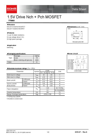
The TT8M3 is a dual N‑channel/P‑channel MOSFET designed for low‑voltage (1.5 V) drive applications. It offers low on‑state resistance, high‑power packaging, and built‑in ESD protection.
The datasheet lists key specifications such as drain‑source voltage, gate‑threshold voltage, on‑state resistance, and total gate charge, along with typical application circuits, measurement setups, and packaging options (tape‑and‑reel, 3000 pieces per unit).
| Maximum Drain‑Source Voltage (VDS) | 20 V |
|---|---|
| Maximum Gate‑Source Voltage (VGS) | +10 V |
| Continuous Drain Current (ID) | 2.5 A |
| On‑State Resistance (RDS(on)) | 65 mΩ (typical) |
| Total Gate Charge (Qg) | 0.6 nC (typical) |
| Power Dissipation | 1.25 W |
| Maximum Channel Temperature | 150 °C |
| Storage Temperature Range | -55 °C to +150 °C |
The TT8M3 can withstand up to 20 V drain‑source voltage.
The gate‑threshold voltage ranges from 0.3 V to 1.0 V.
It is supplied in tape‑and‑reel format, with a basic ordering unit of 3000 pieces.