
ispGDX is a family of high-performance digital crosspoint that features 5V power supply, 5.0ns input-to-output/5.0ns clock-to-output delay, low power consumption, programmable clock, programmable output resistance, etc.
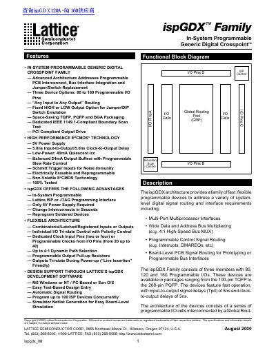
The ispGDX family from Lattice Semiconductor offers in‑system programmable generic digital crosspoints that can route any input to any output, replace jumpers or DIP switches, and support high‑performance E²CMOS technology. Devices are available with 80, 120, or 160 programmable I/O pins in compact TQFP, PQFP, and BGA packages. Key features include a 5 V power supply, 5 ns input‑to‑output and clock‑to‑output delays, 24 mA sink/source output drive, programmable slew‑rate control, Schmitt‑trigger inputs for noise immunity, and full IEEE 1149.1 boundary‑scan test support. The architecture uses a Global Routing Pool (GRP) with per‑pin programmable OE, CLK, and MUX controls, and offers optional dedicated clock pins for minimal latency.
| Supply Voltage | 5 V (typical) |
|---|---|
| Input‑to‑Output Delay | 5.0 ns |
| Clock‑to‑Output Delay | 5.0 ns |
| Quiescent Current | 40 mA |
| Output Drive Capability | 24 mA sink/source per I/O |
| Programmable Slew‑Rate Control | Yes |
| Schmitt‑Trigger Inputs | Yes |
The devices can be programmed via Lattice ISP or JTAG using the dedicated BSCAN/ispEN pin.
Yes, each output can be programmed to a fixed HIGH or LOW level to emulate jumpers or DIP switches.