
ispGDXV™ 3.3V Generic Digital Crosspoint is a high-performance device with a 3.3V core power supply, fast switching speed, low power consumption and broad interface compatibility. It is the ideal choice for Programmable PCB Interconnect, Bus Interface Integration and Jumper/Switch Replacement.
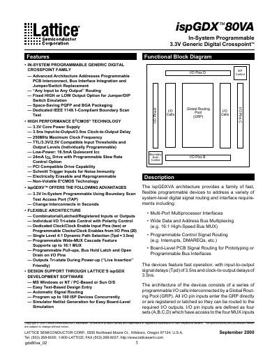
The ispGDX80VA is a 3.3 V in‑system programmable generic digital crosspoint device built with high‑performance E2CMOS technology. It offers 3.5 ns input‑to‑output and clock‑to‑output delays, up to 250 MHz clock frequency, and programmable I/O features such as individual tri‑state control, slew‑rate control, and open‑drain options. The device is available in 100‑pin TQFP, 208‑pin PQFP, and 388‑ball fpBGA packages.
Designed for programmable random signal interconnect, programmable data path, and solid‑state switch replacement applications, the ispGDX80VA supports PCI‑compatible drive capability, boundary‑scan test, and a user‑electronic signature area. It can be programmed via the standard IEEE 1149.1 Test Access Port and retains its configuration without power.
| Core Supply Voltage | 3.3 V |
|---|---|
| Input‑to‑Output Delay | 3.5 ns |
| Maximum Clock Frequency | 250 MHz |
| Output Drive Current | 24 mA sink / 12 mA source |
| Package Options | 100‑Pin TQFP, 208‑Pin PQFP, 388‑Ball fpBGA |
| Erase/Reprogram Cycles | 10,000 cycles |
The device uses a 3.3 V core power supply.
It can operate up to 250 MHz.
Each output can sink up to 24 mA.
Yes, it supports PCI‑compatible drive capability for all I/Os.