
ispGDX TM160V/VA is a family of In-System Programmable 3.3V Generic Digital Crosspoint. Its features include “Any Input to Any Output” Routing, Fixed HIGH or LOW Output Option for Jumper/DIP Switch Emulation, Space-Saving PQFP and BGA Packaging, Dedicated IEEE 1149.1-Compliant Boundary Scan Test, etc.
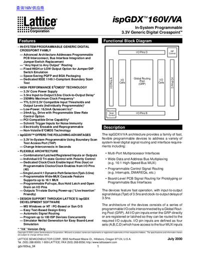
The ispGDX160V/VA family provides a fast, flexible, in‑system programmable routing solution for digital signals. It features a 3.3 V core supply, 3.5 ns input‑to‑output and clock‑to‑output delays, and a maximum clock frequency of 250 MHz. Each I/O pin can be individually programmed for output level, slew rate, pull‑up, and open‑drain operation, and the device supports IEEE 1149.1‑compliant boundary‑scan testing.
The architecture uses a single Global Routing Pool (GRP) with programmable 4:1 multiplexers that can be cascaded to 16:1. Dedicated clock pins, programmable polarity, and non‑volatile E 2CMOS technology enable reliable live‑insertion operation. The device is offered in 208‑pin PQFP and BGA packages and includes security and user‑electronic‑signature features.
| Core Supply Voltage | 3.3 V |
|---|---|
| Input‑to‑Output Delay | 3.5 ns |
| Maximum Clock Frequency | 250 MHz |
| Output Drive Capability | 24 mA sink, 12 mA source |
| Package Types | 208‑Pin PQFP, 208‑Ball BGA, 272‑Ball BGA |
| Quiescent Current | 16.5 mA |
The device operates from a 3.3 V core supply.
The input‑to‑output delay is 3.5 ns.
The maximum clock frequency is 250 MHz.
Outputs can sink 24 mA and source 12 mA at JEDEC LVTTL levels.