
ispLSI®2128V 3.3V High Density Programmable Logic
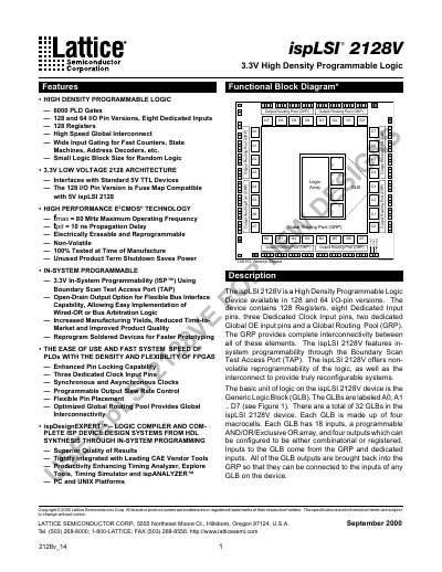
The ispLSI 2128V is a high-density programmable logic device available in 128 and 64 I/O pin versions. It features 6000 PLD gates, 128 registers, and eight dedicated inputs, utilizing 3.3V low-voltage E²CMOS technology for high-speed operation up to 80 MHz.
The device architecture includes Generic Logic Blocks (GLBs) connected via a Global Routing Pool (GRP). It supports in-system programmability (ISP) using the Boundary Scan Test Access Port (TAP), allowing for reprogramming of soldered devices. Outputs can be configured as standard totem-pole or open-drain.
| Maximum Operating Frequency (fmax) | 80 MHz |
|---|---|
| Propagation Delay (tpc) | 10 ns |
| Number of Registers | 128 |
| Data Retention Time | 20 Years |
The maximum operating frequency (fmax) is 80 MHz.
Yes, it interfaces with standard 5V TTL devices and device pins can be safely driven to 5V signal levels.