
This document introduces the Lattice Semiconductor ispClock™5620A In-System-Programmable Analog Circuit usage and features.
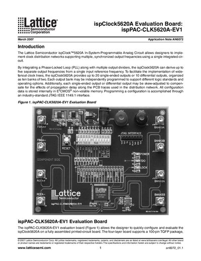
The Lattice ispPAC-CLK5620A-EV1 evaluation board provides a ready‑to‑use platform for evaluating the ispClock5620A PLL‑based clock distribution IC. The board supports a 100‑pin TQFP device, offers up to 20 single‑ended or 10 differential outputs organized in ten banks, and includes SMA connectors, banana‑plug power inputs, and a JTAG programming header.
The document describes the power‑supply options, programming interface via the ispDOWNLOAD cable, dip‑switch configuration for output driver voltages, indicator LEDs, and detailed schematics. Component lists, revision history and technical support contacts are also included.
| Number of single‑ended outputs | 20 |
|---|---|
| Number of differential outputs | 10 |
| Output banks | 10 banks of two |
| Core power supply voltage | 3.3 V |
| Output driver supply options | 1.5 V, 1.8 V, 2.5 V or 3.3 V |
| Board supply voltage range | 4.5 V‑5.5 V |
| On‑board oscillator frequency | 100 MHz |
| Dip‑switch count for VCCO programming | 12‑position |
The board can be powered from a single 4.5 V‑5.5 V supply, either via banana plugs or a 5 mm DC jack.
It provides ten banks of two, supporting up to 20 single‑ended or 10 differential outputs.
Programming is done through the JTAG IEEE 1149.1 interface using the ispDOWNLOAD programming cable connected to a PC parallel port.
Use the 12‑position dip‑switch S2; switch positions 10‑12 select 1.5 V, 1.8 V, 2.5 V or 3.3 V for the VCCO supply.