
ispLSI ® 5256VA In-System Programmable 3.3V SuperWIDE™ High Density PLD is a high-density, high-performance, low-power PLD with 12000 PLD gates/256 macrocells, powered by a 3.3V power supply, supports 3.3V/2.5V selectable I/O, has up to 192 I/O pins, 256 registers, and high-speed global interconnects.
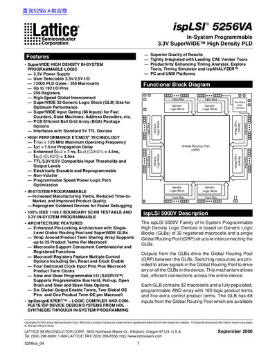
The ispLSI 5256VA is a high-density, in-system programmable logic device (PLD) utilizing 3.3V SuperWIDE technology. It features 12,000 PLD gates and 256 macrocells, operating with a maximum frequency of 125 MHz.
| PLD Gates | 12000 |
|---|---|
| Macrocells | 256 |
| I/O Pins | Up to 192 |
| Registers | 256 |
| Maximum Operating Frequency | 125 MHz |
| Propagation Delay | 7.5 ns |
The device operates from a 3.3V power supply.
Yes, it is in-system programmable for faster debugging and improved product quality.
Yes, it is 100% IEEE 1149.1 Boundary Scan Testable.