
This datasheet provides the specifications of AO4900A, including maximum current, maximum voltage, maximum power dissipation, and maximum temperature.
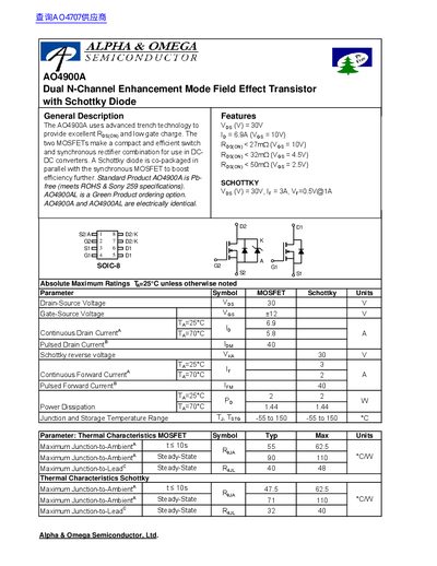
The AO4900A is a dual N‑channel enhancement mode MOSFET that incorporates a Schottky diode in the same package. It is designed for use in DC‑DC converters where low on‑resistance and fast switching are required. The device is RoHS‑compliant and offered in a Pb‑free version.
The datasheet lists absolute maximum ratings, typical electrical characteristics, thermal parameters, and switching performance. Graphs illustrate on‑resistance versus current, gate‑charge curves, and diode forward characteristics, helping designers evaluate the part for efficiency and thermal management in their circuits.
| Maximum Drain‑Source Voltage (VDS) | 30 V |
|---|---|
| Continuous Drain Current (ID) | 6.9 A (VGS = 10 V) |
| On‑Resistance (RDS(ON)) at VGS=10 V | < 27 mΩ |
| On‑Resistance (RDS(ON)) at VGS=4.5 V | < 32 mΩ |
| Schottky Forward Voltage (VF) | 0.45‑0.5 V |
| Input Capacitance (Ciss) | 900‑1100 pF |
| Thermal Resistance Junction‑to‑Ambient (RθJA) | 62.5 °C/W |
The AO4900A can withstand up to 30 V between drain and source.
The on‑resistance is less than 27 mΩ when VGS is 10 V.
It can conduct up to 6.9 A continuously at VGS = 10 V.
The Schottky diode forward voltage is between 0.45 V and 0.5 V.