
AO4610 is a N-channel and P-channel complementary enhancement mode field effect transistor produced by Alpha & Omega Semiconductor, Ltd. Its maximum reverse voltage is 30 V, maximum continuous forward current is 3 A, and maximum continuous drain current is 8.5 A.
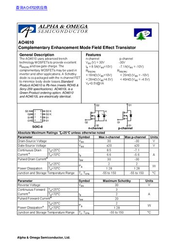
The AO4610 is a complementary enhancement‑mode field‑effect transistor that combines n‑channel, p‑channel and Schottky technologies. It is designed for inverter and other applications, offering low on‑resistance, low gate charge, and a 30 V drain‑source rating.
The document lists absolute maximum ratings, thermal limits, static and dynamic electrical parameters, and switching characteristics. Typical on‑region, transfer, and body‑diode curves are included, along with thermal impedance and single‑pulse power rating graphs.
| Drain‑Source Voltage (VDS) Max | 30 V (positive) / -30 V (negative) |
|---|---|
| Gate‑Source Voltage (VGS) Max | ±20 V |
| Continuous Drain Current (VGS=10 V) | 8.5 A |
| Continuous Drain Current (VGS=-10 V) | 7.1 A |
| Input Capacitance (Ciss) – n‑channel | 1040 pF |
| Input Capacitance (Ciss) – p‑channel | 1573 pF |
| Total Gate Charge (VGS=10 V) | 19.2 nC |
The AO4610 can handle up to 30 V in the positive direction and –30 V in the negative direction.
Yes, the AO4610 is Pb‑free and meets RoHS specifications.
The total gate charge at VGS = 10 V is 19.2 nC.