
The AO4411 is a P-Channel enhancement mode field-effect transistor that uses advanced trench technology to provide excellent RDS(ON) and ultra-low gate charge. It is suitable for use as a load switch or in PWM applications.
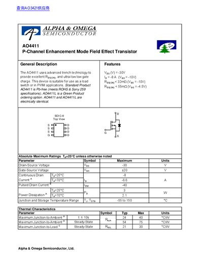
The AO4411 P‑Channel enhancement mode field‑effect transistor uses trench technology to achieve low on‑resistance and low gate charge, making it suitable for load‑switch and PWM applications. The device is Pb‑free, RoHS compliant, and offered in a standard (AO4411) and a green (AO4411L) version that are electrically identical.
Key electrical parameters include a maximum drain‑source voltage of –30 V, continuous drain current of –8 A at 25 °C, and a pulsed drain current rating of –40 A. Thermal characteristics show a typical junction‑to‑ambient thermal resistance of 24 °C/W (steady‑state) and a maximum power dissipation of 2.1 W at 70 °C. Detailed capacitance and gate‑charge data are provided for design calculations.
| Drain‑Source Voltage (VDS) | -30 V |
|---|---|
| Gate‑Source Voltage (VGS) | +20 V |
| Continuous Drain Current (ID) at 25 °C | -8 A |
| Pulsed Drain Current | -40 A |
| Power Dissipation at 70 °C | 2.1 W |
| Typical On‑Resistance (RDS(on)) | 33 mΩ |
| Gate Charge (Qg) at VGS = -10 V | 18.4 nC (typ) |
| Input Capacitance (Ciss) | 920 pF |
| Output Capacitance (Coss) at VGS = 0 V | 190 pF |
| Junction‑to‑Ambient Thermal Resistance (steady‑state, typical) | 24 °C/W |
The AO4411 is rated for a maximum drain‑source voltage of –30 V.
It can conduct up to –8 A continuously at 25 °C.
Yes, the standard AO4411 is Pb‑free and meets RoHS specifications.
The typical on‑resistance is 33 mΩ under those conditions.