
This document describes the features and characteristics of the NTB23N03R power MOSFET, which is designed for low voltage, high-speed switching applications in power supplies, converters, power motor controls, and bridge circuits.
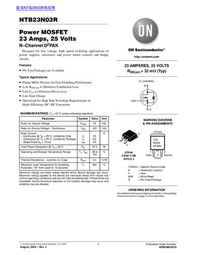
The NTB23N03R is a low‑voltage, high‑speed N‑channel power MOSFET designed for use in power supplies, converters, motor controls and bridge circuits. It features a planar HD3e process, low Rds(on), low input capacitance and low gate charge, making it suitable for high‑efficiency DC‑DC converters.
Key electrical specifications include a 25 V drain‑to‑source rating, ±20 V gate‑to‑source rating, 23 A continuous drain current, typical on‑resistance of 32 mΩ, input capacitance of 225 pF and total gate charge of 3.76 nC. The device is supplied in a D2PAK (TO‑263) package with detailed dimensions and ordering information provided.
| Drain-to-Source Voltage (Vds) | 25 V |
|---|---|
| Gate-to-Source Voltage (Vgs) | ±20 V |
| Continuous Drain Current (Id) | 23 A |
| Typical On‑Resistance (Rds(on)) | 32 mΩ |
| Input Capacitance (Ciss) | 225 pF |
| Total Gate Charge (Qg) | 3.76 nC |
The device can handle up to 23 A continuous drain current (chip limited).
It is supplied in a D2PAK (TO‑263) surface‑mount package.
Typical Rds(on) is 32 mΩ.