
GAL20V8 is a high performance E2CMOS PLD (programmable logic device) launched by Lattice company in August 2006. It has a maximum propagation delay of 5ns, Fmax=166MHz, 4ns maximum from clock input to data output, UltraMOS® Advanced CMOS technology, 50% to 75% lower power consumption, 8 output logic macrocells, preload and power-on reset.
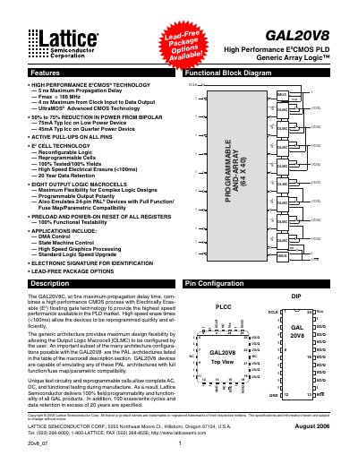
The GAL20V8 is a high‑performance E²CMOS programmable logic device offering up to 166 MHz operation, 5 ns maximum propagation delay, and active pull‑ups on all pins. It supports reconfigurable logic, rapid electrical erasure (<100 ms), and up to 20‑year data retention, making it suitable for DMA control, state machines, and high‑speed graphics processing.
The document provides detailed specifications for commercial and industrial grade packages, pin‑out diagrams for DIP and PLCC formats, and explains the three global Output Logic Macrocell (OLMC) configuration modes—simple, complex, and registered—along with the associated architecture bits and usage restrictions.
| Maximum propagation delay (Tpd) | 5 ns |
|---|---|
| Maximum clock‑to‑data output delay | 4 ns |
| Maximum operating frequency (Fmax) | 166 MHz |
| Typical Icc (Low Power device) | 75 mA |
| Typical Icc (Quarter Power device) | 45 mA |
| Erase/write cycles | 100 cycles |
| Data retention | ≥20 years |
| Registered mode clock pin | Pin 1 (CLK) |
| Registered mode output‑enable pin | Pin 13 (OE) |
The GAL20V8 has a maximum propagation delay of 5 ns.
The device is specified for 100 erase/write cycles.
Pin 1 is permanently configured as the clock (CLK) and Pin 13 as the output‑enable (OE) in registered mode.
The GAL20V8 can operate up to 166 MHz.