
The document introduces version 3.1 released on November 9, 1998, with 7 features. The product series includes XC3000A, XC3000L, XC3100A, and XC3100L. It is suitable for various custom VLSI design tasks, replacing TTL, MSI, and other PLD logic. It adopts high-performance CMOS static memory technology with toggle rates of 70 to 370 MHz and logic delays of 7 to 1.5 ns. The flexible FPGA architecture includes programmable arrays ranging from 1,000 to 7,500 gate complexity, extensive register, combinatorial, and I/O capabilities, high fan-out signal distribution, low-skew clock nets, internal 3-state bus capabilities, TTL or CMOS input thresholds, and an on-chip crystal oscillator amplifier. It supports unlimited reprogrammability for easy design iteration and in-system logic changes. There are over 20 different packaging options, including plastic and ceramic surface-mount and pin-grid-array packages, as well as thin and very thin quad flat pack options. The product is ready for volume production with standard, off-the-shelf availability and 100% factory pre-tested devices. A complete development system is provided, including schematic capture, automatic place and route, logic and timing simulation, interactive design editor for design optimization, timing calculator, and interfaces to popular tools.
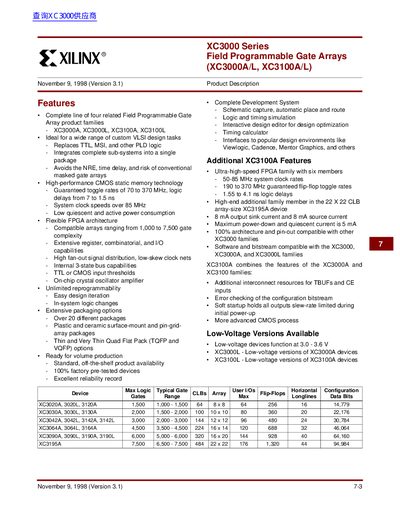
The XC3000 Series Field Programmable Gate Arrays are high‑performance, high‑density digital ICs offering a flexible, user‑programmable architecture. The family includes XC3000A, XC3000L, XC3100A, and XC3100L devices, all sharing a common architecture, development tools, and pin‑out compatibility. They provide a range of logic capacities, package options, and speed grades suitable for custom VLSI design tasks.
The document details the FPGA architecture—perimeter I/O blocks, core configurable logic blocks, and interconnect resources—along with configuration memory design, I/O options, and programmable features such as soft‑startup, slew‑rate control, and voltage thresholds. It also lists key specifications such as toggle rates, logic delays, clock speeds, power consumption, and package varieties.