
This is an introduction to the Xilinx XC5200 FPGA product. It introduces the main features, performance, functions, application scenarios of this product.
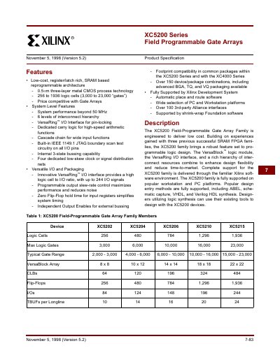
The XC5200 Series Field‑Programmable Gate Arrays are low‑cost, SRAM‑based devices built on a 0.5 µm three‑layer metal CMOS process. They offer 256 to 1,936 logic cells (3,000 to 23,000 gates), system performance beyond 50 MHz, and a rich hierarchy of interconnect resources including six levels of routing hierarchy and the VersaRing I/O interface.
The architecture combines Configurable Logic Blocks (CLBs) with a Local Interconnect Matrix and direct connects to form VersaBlocks. Each CLB contains four Logic Cells with dedicated carry logic, three‑state buffers, and optional flip‑flops or latches. The I/O pins provide programmable slew‑rate control, 8 mA source/sink capability, and built‑in IEEE 1149.1 JTAG boundary‑scan test circuitry.
| Logic Cells | 256 to 1,936 |
|---|---|
| Process Technology | 0.5 µm three‑layer metal CMOS |
| Maximum Clock Speed | Beyond 50 MHz (benchmarked >66 MHz) |
| I/O Pin Current | 8 mA source and sink |
| JTAG Boundary Scan | Built‑in IEEE 1149.1 support on all I/O pins |
| Global Buffers | Four per device |
Devices range from 256 to 1,936 logic cells.
Each I/O pin can source and sink up to 8 mA.
Yes, it includes built‑in IEEE 1149.1 JTAG boundary‑scan test circuitry on all I/O pins.