
The MAX9171/MAX9172 are single/dual low-voltage differential signaling (LVDS) receivers designed for high-speed applications requiring minimum power consumption, space, and noise. Both devices support switching rates exceeding 500Mbps while operating from a single 3.3V supply. The MAX9171 is a single LVDS receiver and the MAX9172 is a dual LVDS receiver. Both devices con- form to the ANSI TIA/EIA-644 LVDS standard and con- vert LVDS to LVTTL/LVCMOS-compatible outputs. A fail-safe feature sets the outputs high when the inputs are undriven and open, terminated, or shorted. The MAX9171/MAX9172 are available in 8-pin SO packages and space-saving thin DFN and SOT23 packages. For lower skew devices, refer to the MAX9111/ MAX9113 data sheet. Applications include multipoint backplane interconnect, laser printers, digital copiers, cellular phone base stations, LCD displays, network switches/routers, and clock distribution.
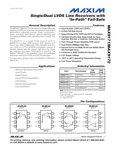
The MAX9171 is a single‑channel LVDS receiver and the MAX9172 is a dual‑channel version. Both devices convert LVDS signals to LVTTL/LVCMOS‑compatible outputs and include an in‑path fail‑safe that forces the output high when inputs are open, undriven, shorted, or terminated. They are designed for high‑speed applications requiring low power, small size, and low noise.
Key features include support for switching rates exceeding 500 Mbps, operation from a single 3.3 V supply, compliance with the ANSI TIA/EIA‑644 LVDS standard, and availability in 8‑pin SO, SOT23, and thin DFN packages. Recommended PCB layout practices, termination requirements, and ESD protection details are also provided.
| Supply Voltage | 3.3 V |
|---|---|
| Operating Temperature Range | -40 °C to +85 °C |
| Maximum Data Rate | >500 Mbps |
| Input Differential Voltage Range | 0.1 V to 1.2 V |
| Package Options | 8‑pin SO, SOT23, thin DFN |
Both devices operate from a single 3.3 V supply.
The fail‑safe drives the output high when the inputs are open, undriven, shorted, or terminated.
They are offered in 8‑pin SO, SOT23, and thin DFN packages.
The receivers support switching rates exceeding 500 Mbps.