
The MAX9156 is an LVPECL-to-LVDS level translator that accepts a single LVPECL input and translates it to a single LVDS output. It is ideal for interfacing between LVPECL and LVDS interfaces in systems that require minimum jitter, noise, power, and space. Ultra-low, 23psp-p added deterministic jitter and 0.6psRMS added random jitter ensure reliable communication in high-speed links that are highly sensitive to timing errors, especially those incorporating clock-and-data recovery, PLLs, serializers, or deserializers. The MAX9156’s switching performance guarantees a 200Mbps data rate, but minimizes radiated noise by guaranteeing 0.5ns minimum output transition time. The MAX9156 operates from a single +3.3V supply and consumes only 10mA supply current over a -40°C to +85°C temperature range. It is available in a tiny 6-pin SC70 package (half the size of a SOT23). Refer to the MAX9155 data sheet for a low-jitter, low-noise LVDS repeater in an SC70 package.
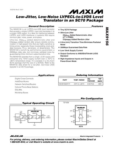
The MAX9156 is a low‑jitter, low‑noise LVPECL‑to‑LVDS level translator that operates from a single +3.3 V supply and consumes only 10 mA. It provides a guaranteed 200 Mbps data rate, 0.5 ns minimum output transition time, and conforms to the ANSI/EIA/TIA‑644 LVDS standard. The device is offered in a compact 6‑pin SC70 package.
The datasheet includes absolute maximum ratings, DC and AC electrical characteristics, typical operating curves, pin descriptions, application guidelines for trace routing and termination, and test circuit diagrams. Ordering information and package dimensions are also provided.
| Supply Voltage | +3.3 V |
|---|---|
| Supply Current (typical) | 10 mA |
| Operating Temperature Range | -40 °C to +85 °C |
| Maximum Data Rate | 200 Mbps |
| Minimum Output Transition Time | 0.5 ns |
| Package | 6‑pin SC70 |
| Output High Voltage (VOH) | 1.6 V |
| Output Low Voltage (VOL) | 0.9 V |
It operates from a single +3.3 V supply.
The device guarantees a 200 Mbps data rate.
Typical supply current is 10 mA.
It is available in a 6‑pin SC70 package.