
The MAX9129 is a quad bus low-voltage differential signaling (BLVDS) driver with flow-through pinout. This device is designed to drive a heavily loaded multipoint bus with controlled transition times (1ns 0% to 100% minimum) for reduced reflections. The MAX9129 accepts four LVTTL/LVCMOS input levels and translates them to output levels of 250mV to 450mV (standard LVDS levels) into a 27Ω load at speeds up to 200Mbps (100MHz). The power-on reset ensures that all four outputs are disabled and high impedance during power up and power down. The outputs can be set to high impedance by two enable inputs, EN and EN, thus dropping the device to a low-power state of 11mW. The enables are common to all four drivers. The flow-through pinout simplifies PC board layout and reduces crosstalk by keeping the LVTTL/LVCMOS inputs and BLVDS outputs separated. The MAX9129 operates from a single +3.3V supply and is specified for operation from -40°C to +85°C. It is available in 16-pin QFN and TSSOP packages. Refer to the MAX9121 data sheet for a quad LVDS line receiver with flow-through pinout.
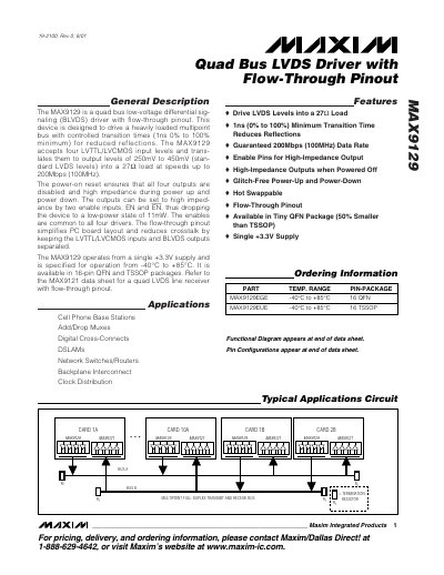
The MAX9129 is a quad‑bus low‑voltage differential signaling (BLVDS) driver designed for heavily loaded multipoint backplane applications. It accepts four LVTTL/LVCMOS inputs and translates them to standard LVDS output levels of 250 mV to 450 mV into a 27 Ω load, operating from a single +3.3 V supply and a temperature range of –40 °C to +85 °C.\n\nKey features include a minimum 1 ns (0%‑to‑100%) transition time, guaranteed 200 Mbps (100 MHz) data rate, enable pins for high‑impedance output, hot‑swappable operation, and flow‑through pinout that simplifies PCB layout and reduces crosstalk. Typical applications are cell‑phone base stations, DSLAMs, network switches/routers, backplane interconnects, and clock distribution.
| Data Rate | 200 Mbps (100 MHz) |
|---|---|
| Transition Time | 1 ns (0%‑to‑100%) minimum |
| Supply Voltage | +3.3 V (single supply) |
| Operating Temperature | -40 °C to +85 °C |
| Load Impedance | 27 Ω |
| Power‑off Consumption | 11 mW |
| Output Voltage Levels | 250 mV to 450 mV |
The MAX9129 supports up to 200 Mbps (100 MHz) data rate.
It operates from a single +3.3 V supply.
The device has a minimum transition time of 1 ns (0%‑to‑100%).
It is designed to drive a 27 Ω load.