
The MAX9159 is a dual low-voltage differential signaling (LVDS) receiver ideal for applications requiring high speed, low power, and low noise.
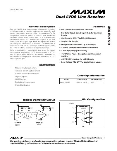
The MAX9159 is a dual low‑voltage differential signaling (LVDS) receiver designed for high‑speed, low‑power applications. It is pin‑compatible with the SN65LVDS9637 and conforms to the ANSI TIA/EIA‑644 LVDS standard, converting LVDS inputs to LVTTL‑compatible outputs.
The device operates from a 3.0 V to 3.6 V supply, supports data rates up to 400 Mbps, and includes a fail‑safe circuit that forces the output high when inputs are undriven, open, terminated, or shorted. It is offered in an 8‑pin SO package and is rated for -40 °C to +85 °C operation.
| Supply Voltage (VCC) | 3.0 V to 3.6 V |
|---|---|
| Data Rate | up to 400 Mbps |
| Propagation Delay (typical) | 2.2 ns |
| Power Dissipation (typical, 200 MHz) | 41 mW |
| ESD Protection | ±8 kV |
| Operating Temperature Range | -40 °C to +85 °C |
| Package | 8‑pin SO |
| Differential Input Threshold | ±100 mV (max) |
The device operates from 3.0 V to 3.6 V.
The receiver is designed for data rates up to 400 Mbps.