
The MAX9181 is an LVPECL-to-LVDS level translator that accepts a single LVPECL input and translates it to a single LVDS output. It is ideal for interfacing between LVPECL and LVDS interfaces in systems that require minimum jitter, noise, power, and space. Ultra-low, 23psP-P added deterministic jitter and 0.6psRMS added random jitter ensure reliable commu- nication in high-speed links that are highly sensitive to timing errors, especially those incorporating clock-and- data recovery, PLLs, serializers, or deserializers. The MAX9181’s switching performance guarantees a 400Mbps data rate, but minimizes radiated noise by guaranteeing 0.5ns minimum output transition time. The MAX9181 operates from a single 3.3V supply and consumes only 10mA supply current over a -40°C to +85°C temperature range. It is available in a tiny 6-pin SC70 package (half the size of a SOT23). Refer to the MAX9180 data sheet for a low-jitter, low-noise LVDS repeater in an SC70 package.
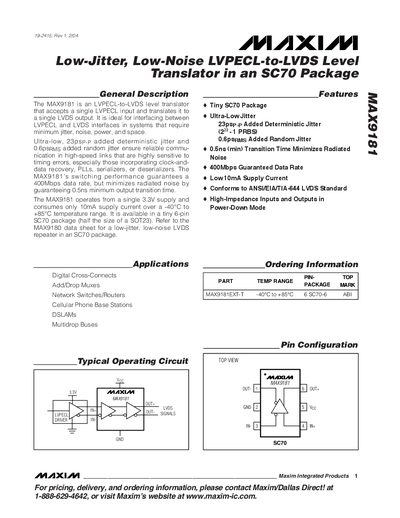
The MAX9181 is a LVPECL‑to‑LVDS level translator that converts a single LVPECL input to a single LVDS output. It is designed for high‑speed links that require minimal jitter, low noise, low power consumption, and a very small footprint.
The device operates from a 3.3 V supply, draws about 10 mA, and guarantees a 400 Mbps data rate with a minimum 0.5 ns output transition time. It is offered in a 6‑pin SC70 package and includes features such as ultra‑low deterministic (23 ps p‑p) and random (0.6 ps p‑p) jitter, high‑impedance inputs/outputs in power‑down mode, and compliance with the ANSI/TIA‑644 LVDS standard.
| Guaranteed Data Rate | 400 Mbps |
|---|---|
| Minimum Transition Time | 0.5 ns |
| Deterministic Jitter | 23 ps p‑p |
| Random Jitter | 0.6 ps p‑p |
| Package | 6‑pin SC70 |
It guarantees a data rate of 400 Mbps.
The device is offered in a tiny 6‑pin SC70 package.
The minimum transition time is 0.5 ns.