
The MAX9179 is a quad low-voltage differential signaling (LVDS) line receiver designed for applications requiring high data rates, low power dissipation, and noise immunity. The receiver accepts four LVDS input signals and translates them to 3.3V LVCMOS output lev- els at speeds up to 400Mbps. The receiver features built-in hysteresis, which improves noise immunity and prevents multiple switching on slow transitioning inputs. The device supports a wide 0.038V to 2.362V common- mode input voltage range, allowing for ground potential differences and common-mode noise between the driver and the receiver. A fail-safe circuit sets the output high when the input is open, undriven and shorted, or undriven and terminated. Common enable inputs control the high- impedance outputs. The MAX9179 has a flow-through pinout for easy PC board layout, and is pin compatible with the MAX9121 and the DS90LV048A with the additional features of high ESD tolerance and built-in hysteresis. The MAX9179 operates from a single 3.3V supply, and is specified for operation from -40°C to +85°C. The device is offered in 16-pin TSSOP and thin QFN packages. Applications include Laser Printers, Digital Copiers, Cell-Phone Base Stations, Telecom Switching Equipment, LCD Displays, Network Switches/Routers, Backplane Interconnect, and Clock Distribution.
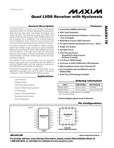
The MAX9179 quad LVDS receiver translates four LVDS inputs to 3.3 V LVCMOS outputs at speeds up to 400 Mbps. It features built‑in hysteresis for noise immunity, a fail‑safe circuit that forces the output high on open or shorted inputs, and high ESD tolerance.
The device operates from a single 3.3 V supply, is specified for –40 °C to +85 °C, and is available in 16‑pin TSSOP and thin QFN packages. Recommended layout includes flow‑through pinout, controlled‑impedance differential traces, and proper power‑supply bypassing.
| Maximum Data Rate | 400 Mbps |
|---|---|
| Supply Voltage | 3.3 V (single supply) |
| Operating Temperature Range | -40 °C to +85 °C |
| Package Types | 16‑pin TSSOP, thin QFN |
| Hysteresis | 50 mV (typ) |
| ESD Tolerance | IEC61000‑4‑2 Level 4 |
The MAX9179 supports a guaranteed data rate of 400 Mbps.
It operates from a single 3.3 V supply.
The built‑in hysteresis is typically 50 mV.
The part is offered in 16‑pin TSSOP and thin QFN packages.