
MAX9173 quad low-voltage differential signaling (LVDS) line receiver with flow-through pinout and “In-Path” Fail-Safe
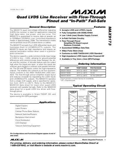
The MAX9173 quad low‑voltage differential signaling (LVDS) line receiver is designed for high‑speed, low‑power applications. It accepts four LVDS differential inputs and converts them to LVCMOS/LVTTL outputs, operating from a single 3.3 V supply and a temperature range of –40 °C to +85 °C. The device includes a flow‑through pinout that simplifies board layout and reduces crosstalk, and an in‑path fail‑safe circuit that forces the output high when inputs are open, undriven and shorted, or undriven and terminated.
Typical applications include digital copiers, laser printers, cellular phone base stations, network switches/routers, backplane interconnects, clock distribution, LCD displays, and telecom switching equipment. The datasheet provides detailed electrical characteristics, pin descriptions, package options, and layout recommendations for optimal LVDS performance.
| Maximum Data Rate | up to 500 Mbps (250 MHz) |
|---|---|
| Supply Voltage | 3.3 V |
| Operating Temperature Range | -40 °C to +85 °C |
| Package Types | 16‑pin TSSOP, 16‑pin SO, 16‑pin Thin QFN |
The fail‑safe drives the receiver output high when the differential input is open, undriven and shorted, or undriven and terminated.
It is offered in 16‑pin TSSOP, 16‑pin SO, and a thin 16‑pin QFN package.
All channels can switch up to 250 MHz.