
The MAX9323 is a low-skew, low-jitter clock and data driver that distributes one of two single-ended LVCMOS inputs to four differential LVPECL outputs. The device operates from 3.0V to 3.6V and consumes only 25mA (max) of supply current, making it ideal for 3.3V systems. It features low 150ps part-to-part skew, low 11ps output-to-output skew, and low 1.7ps RMS jitter, making it suitable for clock and data distribution across a backplane or board. The MAX9323 is pin compatible with the ICS8535-01 and is available in space-saving TSSOP and thin QFN packages. It is suitable for precision clock distribution, low-jitter data repeaters, data and clock drivers, and buffers in various applications.
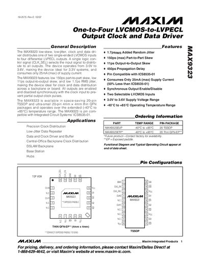
The MAX9323 is a low‑skew, low‑jitter clock and data driver that distributes one of two single‑ended LVCMOS inputs to four differential LVPECL outputs. A single control signal (CLK_SEL) selects the active input, and the device operates from 3.0 V to 3.6 V, drawing only up to 25 mA of supply current.
Key features include 150 ps maximum part‑to‑part skew, 11 ps output‑to‑output skew, 1.7 ps RMS jitter, and operation over an extended temperature range of –40 °C to +85 °C. The device is offered in 20‑pin TSSOP and ultra‑small 20‑pin thin QFN packages and is pin‑compatible with the ICS8535‑01.
| Supply Voltage Range | 3.0 V to 3.6 V |
|---|---|
| Maximum Supply Current | 25 mA (max) |
| Part‑to‑Part Skew | 150 ps (max) |
| Output‑to‑Output Skew | 11 ps |
| RMS Jitter | 1.7 ps |
| Propagation Delay | 450 ps |
| Output Rise Time | 100 ps typical (20%‑80%) |
| Operating Temperature Range | -40 °C to +85 °C |
| Package Types | 20‑pin TSSOP, 20‑pin Thin QFN (4 mm × 4 mm) |
It operates from 3.0 V to 3.6 V.
The maximum supply current is 25 mA.
The part‑to‑part skew is specified as 150 ps maximum.