
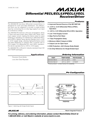
The MAX9321B low-skew differential receiver/driver is designed for clock and data distribution. The differential input can be adapted to accept a single-ended input by connecting the on-chip VBB supply to an input as a reference voltage. The MAX9321B features ultra-low propagation delay (172ps) and part-to-part skew (20ps) with 24mA maximum supply current, making this device ideal for clock buffering or repeating. For interfacing to differential PECL and LVPECL signals, these devices operate over a +3.0V to +5.5V supply range, allowing high-performance clock and data distribution in systems with a nominal 3.3V or 5.0V supply. For differential ECL and LVECL operation, this device operates from a -3.0V to -5.5V supply. The MAX9321B is offered in industry-standard 8-pin SO and TSSOP packages.
The MAX9321B low‑skew differential receiver/driver is designed for high‑performance clock and data distribution. It can accept single‑ended inputs by using the on‑chip VBB reference and supports both PECL/LVPECL (+3.0 V to +5.5 V) and ECL/LVECL (‑3.0 V to ‑5.5 V) operation.
Key specifications include an ultra‑low propagation delay of 172 ps, part‑to‑part skew of 20 ps, and a typical supply current of 24 mA. The device is offered in 8‑pin SO and TSSOP packages, with recommended 50 Ω termination for the differential outputs. It features ESD protection above 2 kV and includes on‑chip reference circuitry for single‑ended operation.
| Positive supply voltage range | +3.0 V to +5.5 V |
|---|---|
| Negative supply voltage range | ‑3.0 V to ‑5.5 V |
| ESD protection (HBM) | >2 kV |
| Output low for open input | Enabled |
| Package options | 8‑pin SO, 8‑pin TSSOP |
The device is offered in 8‑pin SO and 8‑pin TSSOP packages.
Terminate each output with a 50 Ω resistor to VCC‑2 V (or an equivalent Thevenin termination).