
The MAX9310A is a fast, low-skew 1:5 differential driver with selectable LVPECL inputs and LVDS outputs, designed for clock distribution applications. This device features an ultra-low propagation delay of 340ps with 48mA of supply current. The MAX9310A operates from a 3V to 3.6V power supply for use in 3.3V systems. A 2:1 input multiplexer is used to select one of two differential inputs. The input selection is controlled through the CLKSEL pin. This device features a synchronous enable function. The MAX9310A LVPECL inputs can be driven by either a differential or single-ended signal. A VBB reference voltage output is provided for use with single-ended inputs. The device can also accept differential HSTL signals. The MAX9310A is offered in a space-saving 20-pin TSSOP package and operates over the extended temperature range from -40°C to +85°C. Applications Data and Clock Drivers and Buffers Central-Office Backplane Clock Distribution DSLAM Base Stations ATE Features Guaranteed 1.0GHz Operating Frequency 8.0ps Output-to-Output Skew 340ps Propagation Delay Accepts LVPECL and Differential HSTL Inputs Synchronous Output Enable/Disable Two Selectable Differential Inputs 3V to 3.6V Supply Voltage On-Chip Reference for Single-Ended Operation ESD Protection: ±2kV (Human Body Model) Input Bias Resistors Drive Output Low for Open Inputs
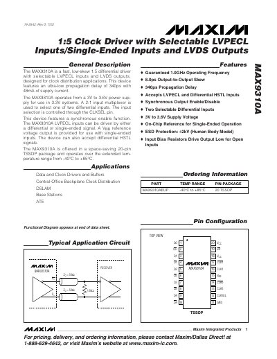
The MAX9310A is a high‑speed, low‑skew 1:5 differential clock driver designed for clock distribution applications. It offers selectable LVPECL inputs, LVDS outputs, an ultra‑low propagation delay of 340 ps, and synchronous enable control.
The device operates from a 3 V to 3.6 V supply, is packaged in a 20‑pin TSSOP, and functions over an extended temperature range of –40 °C to +85 °C. Detailed electrical characteristics, pin descriptions, and application guidelines are provided in the datasheet.
| Propagation delay | 340 ps |
|---|---|
| Output‑to‑Output Skew | 8 ps |
| Operating frequency | 1.0 GHz |
| Supply voltage range | 3 V to 3.6 V |
| Package | 20‑pin TSSOP |
| Operating temperature range | -40 °C to +85 °C |
The MAX9310A has an ultra‑low propagation delay of 340 ps.
It operates from a 3 V to 3.6 V power supply.
The device is guaranteed to operate up to 1.0 GHz.
It is supplied in a 20‑pin TSSOP package.