
The MAX9160 is a 125MHz, 14-port LVTTL/LVCMOS clock driver that repeats the selected LVDS or LVTTL/LVCMOS input on two output banks. Each bank consists of seven LVTTL/LVCMOS series terminated outputs and a bank enable. The LVDS input has a fail-safe function. The MAX9160 has a propagation delay that can be adjusted using an external resistor to set the bias current for an internal delay cell. The LVTTL/LVCMOS outputs feature 200ps maximum output-to-output skew and ±100ps maximum peak-to-peak jitter. The MAX9160 is designed to operate with a 3.3V supply voltage over the extended temperature range of -40°C to +85°C. This device is available in 28-pin exposed- and nonexposed-pad TSSOP and 32-lead 5mm x 5mm QFN packages.
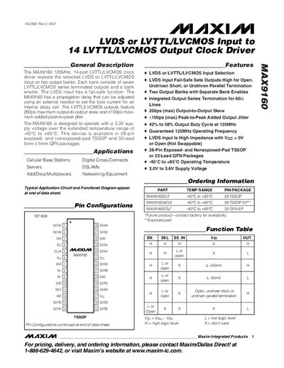
The MAX9160 clock driver repeats a selected LVDS or LVTTL/LVCMOS input on two banks of seven LVTTL/LVCMOS outputs. Each output bank has an enable line, and the device includes a fail‑safe circuit that forces outputs high when the LVDS input is open, undriven short, or undriven terminated. Propagation delay can be tuned with an external resistor.
The device operates from a 3.0 V to 3.6 V supply over an extended temperature range of –40 °C to +85 °C and is offered in 28‑pin TSSOP and 32‑lead QFN packages. Key performance figures include 200 ps maximum output‑to‑output skew, +100 ps maximum added jitter, and a guaranteed 125 MHz operating frequency.
| Supply Voltage | 3.0 V to 3.6 V |
|---|---|
| Operating Temperature | -40 °C to +85 °C |
| Number of Outputs | 14 LVTTL/LVCMOS |
| Output Skew | 200 ps max |
| Added Output Jitter | +100 ps max |
| Output Duty Cycle | 42 % to 58 % at 125 MHz |
| Package Types | 28‑Pin TSSOP, 32‑Lead QFN |
| Maximum Operating Frequency | 125 MHz (guaranteed) |
The fail‑safe circuit sets enabled outputs high when the LVDS input is open, undriven short, or undriven terminated.
The MAX9160 is guaranteed to operate at 125 MHz.
It operates from 3.0 V to 3.6 V.
The maximum output‑to‑output skew is 200 ps.