
The MAX9315 is a low-skew, 1-to-5 differential driver designed for clock and data distribution. This device allows selection between two inputs. The selected input is reproduced at five differential outputs. The differential inputs can be adapted to accept a single-ended input by connecting the on-chip VBB supply to one input as a reference voltage. The MAX9315 features low output-to-output skew (20ps), making it ideal for clock and data distribution across a backplane or a board. For interfacing to differential HSTL and LVPECL signals, this device operates over a +2.375V to +3.8V supply range, allowing high-performance clock or data distribution in systems with a nominal +2.5V or +3.3V supply. For differential LVECL operation, this device operates with a -2.375V to -3.8V supply. The MAX9315 is offered in a space-saving 20-pin TSSOP package.
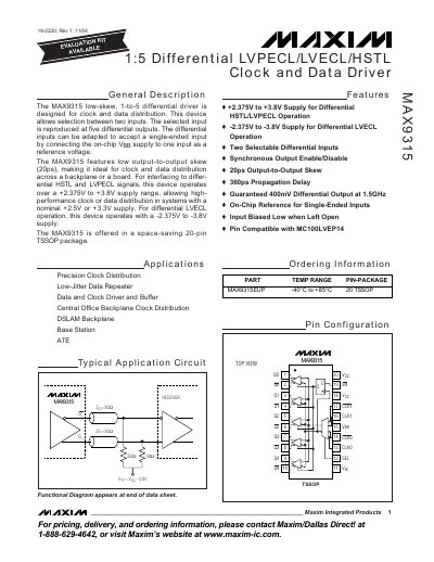
The MAX9315 low‑skew, 1‑to‑5 differential driver is designed for clock and data distribution, supporting two selectable differential inputs and reproducing the selected input on five differential outputs. It operates from +2.375 V to +3.8 V for HSTL/LVPECL or –2.375 V to –3.8 V for LVECL, and features a 20 ps output‑to‑output skew.
The device is supplied in a space‑saving 20‑pin TSSOP package, includes synchronous enable/disable, and provides guaranteed 400 mV differential output at 1.5 GHz. Detailed electrical characteristics, pin functions, and application notes are provided for board‑level integration.
| Supply voltage (HSTL/LVPECL) | +2.375 V to +3.8 V |
|---|---|
| Supply voltage (LVECL) | -2.375 V to -3.8 V |
| Number of differential outputs | 5 |
| Output‑to‑output skew | 20 ps |
| Propagation delay | 360 ps (typical) |
| Differential output voltage (min) | ≥ 400 mV at 1.5 GHz |
The MAX9315 provides five differential outputs (Q0–Q4).
It requires a supply voltage between +2.375 V and +3.8 V.
The typical output‑to‑output skew is 20 ps.
The typical propagation delay is 360 ps.