
The MAX9317/MAX9317A/MAX9317B/MAX9317C are low-skew, dual 1-to-5 differential drivers designed for clock and data distribution. They reproduce the differential input at five LVDS outputs with a low output-to-output skew of 5ps. The MAX9317/MAX9317A are designed for low-voltage operation from a 2.375V to 2.625V power supply for use in 2.5V systems. The MAX9317B/MAX9317C operate from a 3.0V to 3.6V power supply for use in 3.3V systems. The MAX9317A/MAX9317C feature 50Ω input termination resistors to reduce component count. The MAX9317 family is available in 32-pin 7mm ✕ 7mm TQFP and space-saving 5mm ✕ 5mm QFN packages and operate across the extended temperature range of -40°C to +85°C.
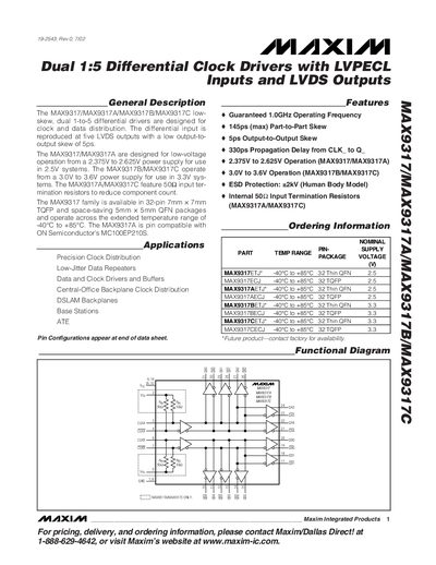
The MAX9317 family provides low‑skew, dual 1‑to‑5 differential drivers for clock and data distribution. Each device accepts LVPECL or LVDS inputs and reproduces the signal on five LVDS outputs with very low output‑to‑output skew.
The devices operate from 2.375‑2.625 V (MAX9317/MAX9317A) or 3.0‑3.6 V (MAX9317B/MAX9317C) supplies, support up to 1 GHz operation, and include on‑chip 50 Ω input termination for LVPECL configurations. Detailed electrical characteristics, pin descriptions, and package information are provided.
| Operating Frequency | 1.0 GHz |
|---|---|
| Output‑to‑Output Skew | 5 ps |
| Part‑to‑Part Skew | 145 ps (max) |
| Propagation Delay (CLK→Q) | 330 ps |
| Supply Voltage (MAX9317 / MAX9317A) | 2.375 V to 2.625 V |
| Supply Voltage (MAX9317B / MAX9317C) | 3.0 V to 3.6 V |
| ESD Protection (Human Body Model) | +2 kV |
The MAX9317 family is guaranteed to operate up to 1.0 GHz.
The output‑to‑output skew is specified as 5 ps.
MAX9317 and MAX9317A run from 2.375 V to 2.625 V, while MAX9317B and MAX9317C run from 3.0 V to 3.6 V.