
MAX9324 is a low-skew, low-jitter, clock and data driver that distributes a differential LVPECL input to four differential LVPECL outputs and one single-ended LVCMOS output. When the differential inputs are equal to GND or are left open, all outputs default to logic low. The MAX9324 operates from 3.0V to 3.6V, making it ideal for 3.3V systems, and consumes only 25mA (max) of supply current. The MAX9324 features low 150ps (max) part-to-part skew, low 15ps output-to-output skew, and low 1.7ps RMS jitter, making the device ideal for clock and data distribution across a backplane or board. CLK_EN and SEOUT_Z control the status of the various outputs. Asserting CLK_EN low configures the differential (Q_, Q_) outputs to a differential low condition and SEOUT to a single-ended logic-low state. CLK_EN operation is synchronous with the CLK_ inputs. A logic high on SEOUT_Z places SEOUT in a high-impedance state. SEOUT_Z is asynchronous with the CLK (CLK) inputs. The MAX9324 is available in space-saving 20-pin TSSOP and ultra-small 20-pin 4mm × 4mm thin QFN packages and operates over the extended (-40°C to +85°C) temperature range. Applications Precision Clock Distribution Low-Jitter Data Repeater Data and Clock Driver and Buffer Central-Office Backplane Clock Distribution DSLAM Backplane Base Station ATE Features o 15ps Differential Output-to-Output Skew o 1.7psRMS Added Random Jitter o 150ps (max) Part-to-Part Skew o 450ps Propagation Delay o Synchronous Output Enable/Disable
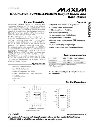
The MAX9324 is a low‑skew, low‑jitter clock and data driver that distributes a differential LVPECL input to four differential LVPECL outputs and a single‑ended LVCMOS output. It operates from 3.0 V to 3.6 V, consumes up to 25 mA, and is suited for 3.3 V systems. Key features include 150 ps part‑to‑part skew, 15 ps output‑to‑output skew, and 1.7 ps RMS jitter, making it ideal for precision clock distribution and data repeater applications.
The datasheet provides absolute maximum ratings, DC and AC electrical characteristics, pin descriptions, timing diagrams, and detailed package information for the 20‑pin TSSOP and 20‑pin thin QFN options. Guidance on power‑supply bypassing, PCB trace design, and output termination is also included.
| Supply Voltage Range | 3.0 V to 3.6 V |
|---|---|
| Operating Temperature Range | -40 °C to +85 °C |
| Part‑to‑Part Skew | 150 ps (max) |
| Output‑to‑Output Skew | 15 ps (max) |
| RMS Jitter | 1.7 ps |
| Propagation Delay | 450 ps (typical) |
| Supply Current | 25 mA (max) |
| Differential Output Frequency | up to 800 MHz |
| Single‑Ended Output Frequency | up to 200 MHz |
| Package Options | 20‑pin TSSOP, 20‑pin Thin QFN (4 mm × 4 mm) |
The device operates from 3.0 V to 3.6 V.
It provides four differential LVPECL outputs and one single‑ended LVCMOS output.
The differential LVPECL outputs can operate up to 800 MHz.
The part is offered in a 20‑pin TSSOP and a 20‑pin thin QFN (4 mm × 4 mm) package.