
This document describes the features and characteristics of Xilinx Virtex-II products, including IP-Immersion™ architecture, SelectRAM™ memory hierarchy, arithmetic functions, flexible logic resources, and high-performance clock management circuitry.
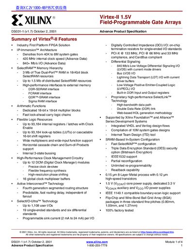
The Virtex-II 1.5V family provides a platform FPGA solution ranging from 40 K to 8 M system gates, supporting high‑performance interfaces such as PCI‑X, LVDS, DDR, and QDR‑SRAM. Key features include up to 12 Digital Clock Manager (DCM) modules, SelectRAM™ memory hierarchy, dedicated 18 × 18 multiplier blocks, and a flexible I/O suite with up to 1,108 user pins.
The devices are fabricated in a 0.15 µm/0.12 µm CMOS 8‑layer metal process and offered in various BGA packages (wire‑bond and flip‑chip) with pitches from 0.80 mm to 1.27 mm. The datasheet also covers configuration modes, boundary‑scan support, read‑back capabilities, and the Integrated Logic Analyzer for in‑system debugging.
| Core supply voltage | 1.5 V |
|---|---|
| Process technology | 0.15 µm / 0.12 µm CMOS 8‑layer metal |
| Maximum internal clock speed | 420 MHz |
| Maximum I/O pins | 1,108 |
| Maximum DCM modules | 12 |
| Density range | 40 K – 8 M system gates |
The Virtex‑II devices operate with a 1.5 V core supply (Vocint).
Each Virtex‑II FPGA can include up to 12 DCM modules.
The XC2V8000 flip‑chip package provides up to 1,108 user I/O pins.
The datasheet lists a maximum internal clock speed of 420 MHz.