
IDT49FCT805BT/CT is a high-speed CMOS buffer/clock driver with extremely low output distortion, low power, high drive capability and high reliability.
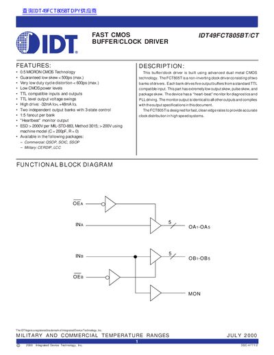
The IDT49FCT805BT/CT is a fast CMOS buffer/clock driver built with 0.5 µm dual‑metal CMOS technology. It offers very low skew (< 500 ps), low duty‑cycle distortion, and high drive capability of –32 mA to +48 mA per output. The device includes a heartbeat monitor output for diagnostics and supports TTL‑compatible inputs and outputs.
The datasheet details pin configurations, absolute maximum ratings, electrical characteristics, power‑supply behavior, and switching performance across commercial (0 °C‑70 °C) and military (‑55 °C‑125 °C) temperature ranges. Package options include QSOP, SOIC, SSOP for commercial use and CERDIP, LCC for military applications.
| Technology | 0.5 µm CMOS |
|---|---|
| Output Skew (max) | < 500 ps |
| Drive Current | -32 mA to +48 mA |
| Temperature Range (commercial) | 0 °C to +70 °C |
| Temperature Range (military) | -55 °C to +125 °C |
| Available Packages | QSOP, SOIC, SSOP, CERDIP, LCC |
The device can source up to +48 mA and sink up to –32 mA per output.
It operates from 0 °C to +70 °C in commercial applications and from –55 °C to +125 °C in military applications.
The part is offered in QSOP, SOIC, SSOP for commercial use and in CERDIP and LCC for military use.
The monitor output is identical to all other outputs and is used for diagnostics.