
ADCLK954 Rev. B is a low jitter clock fanout buffer, which features 2 selectable differential inputs, 12 LVPECL outputs, 4.8 GHz operating frequency, 75 fs rms broadband random jitter, and 3.3 V power supply.
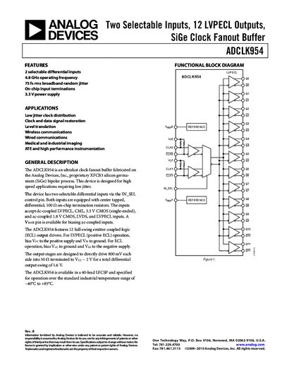
The ADCLK954 clock fanout buffer from Analog Devices provides two selectable differential inputs and twelve LVPECL outputs. It is fabricated on a proprietary SiGe bipolar process and is intended for low‑jitter clock distribution, signal restoration, level translation, and high‑performance instrumentation.
The device is supplied in a 40‑lead LFCSP package, operates over a –40 °C to +85 °C temperature range, and requires a 3.3 V supply. Detailed electrical characteristics, pin descriptions, and layout guidelines are included for designers.
| Operating Frequency | 4.8 GHz |
|---|---|
| Broadband Random Jitter | 75 fs rms |
| Supply Voltage | 3.3 V (2.97‑3.63 V) |
| Output Differential Swing | 1.6 V |
| Temperature Range | -40 °C to +85 °C |
| Package | 40‑lead LFCSP |
The device can operate up to 48 GHz output frequency.
It requires a 3.3 V supply, with a nominal range of 2.97 V to 3.63 V.
The ADCLK954 operates from –40 °C to +85 °C.
It provides twelve full‑swing LVPECL output drivers.