
AD9515 is a low jitter, low phase noise clock distribution IC that features programmable dividers, coarse delay adjustment and 1.6 GHz LVPECL, 800 MHz/250 MHz LVDS/CMOS clock outputs. It can provide low jitter and low phase noise clock signals to high performance ADC, DAC, DDS, DDC, DUC and MxFE applications.
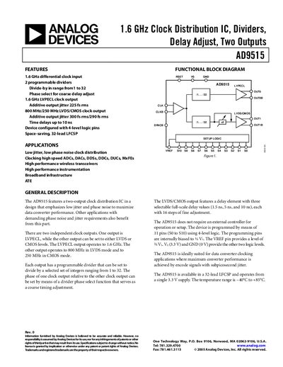
The AD9515 is a two‑output clock distribution integrated circuit designed for low jitter and low phase‑noise applications. It features a 1.6 GHz differential LVPECL output and a second output selectable as LVDS (up to 800 MHz) or CMOS (up to 250 MHz), each with programmable integer dividers from 1 to 32 and coarse phase‑adjust capability.
Typical applications include high‑speed data‑converter clocking, wireless transceivers, instrumentation, and broadband infrastructure. The device is supplied in a 32‑lead LFCSP package and operates from a single 3.3 V supply over a temperature range of –40 °C to +85 °C.
| Maximum input frequency | 1.6 GHz |
|---|---|
| Input sensitivity (single‑ended) | 150 mV p‑p |
| LVPECL additive output jitter | 225 fs rms |
The AD9515 can accept clock inputs up to 1.6 GHz.
It provides one LVPECL output and a second output that can be configured as LVDS or CMOS.
The LVPECL output has an additive jitter of 225 fs rms.
The device operates from a single 3.3 V supply.