
The AD9517-1 is a 12-output clock generator with an integrated 2.5 GHz VCO. The clock generator features a low phase noise, phase-locked loop (PLL). The AD9517-1 supports 1 differential or 2 single-ended reference inputs and has reference monitoring capability. In addition, the clock generator supports automatic revertive and manual reference switchover/holdover modes and accepts LVPECL, LVDS or CMOS references to 250 MHz. The AD9517-1 has a programmable delay path to the PFD and supports digital or analog lock detect. The clock generator has 2 pairs of 1.6 GHz LVPECL outputs, each output pair shares a 1:32 divider with coarse phase delay. Additive output jitter is 225 fs rms, channel-to-channel skew paired outputs are <10 ps. The AD9517-1 also has 2 pairs of 800 MHz LVDS clock outputs, each output pair shares two cascaded 1:32 dividers with coarse phase delay. Additive output jitter is 275 fs rms, fine delay adjust (Δt) is supported on each LVDS clock output.
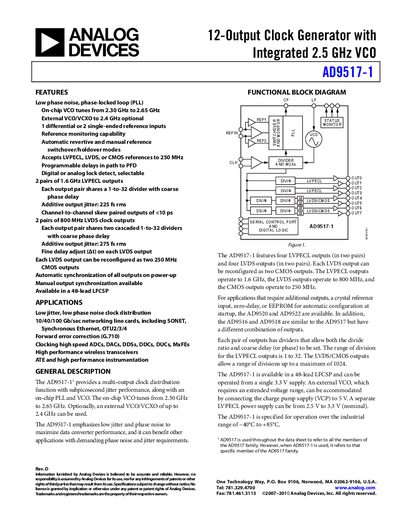
The AD9517-1 is a 12‑output clock generator with an integrated 2.5 GHz VCO, offering low phase‑noise and low jitter performance for high‑speed data converters, networking, and wireless applications. It supports LVPECL, LVDS, and CMOS output formats with programmable dividers and fine‑delay adjustments.
The document provides full electrical specifications, power‑supply requirements, PLL characteristics, clock input and output parameters, timing characteristics, and package information, along with application notes and ordering details.
| Supply voltage (Vs) | 3.3 V |
|---|---|
| On‑chip VCO frequency range | 2.30–2.65 GHz |
| LVPECL output maximum frequency | 2.95 GHz |
| LVDS output frequency | 800 MHz |
| CMOS output frequency | 250 MHz |
| Operating temperature range | -40 °C to +85 °C |
| Package | 48‑Lead LFCSP |
The on‑chip VCO tunes from 2.30 GHz to 2.65 GHz.
It provides two pairs (four outputs) of LVPECL and two pairs (four outputs) of LVDS.
The device operates from a 3.3 V supply (typical 3.3 V, range 3.135–3.465 V).
The AD9517‑1 is specified for –40 °C to +85 °C.