
BSP171P SIPMOS® Small-Signal-Transistor Features P-Channel, Enhancement mode, Logic level, Avalanche rated, dv/dt rated, Pb-free lead plating; RoHS compliant.
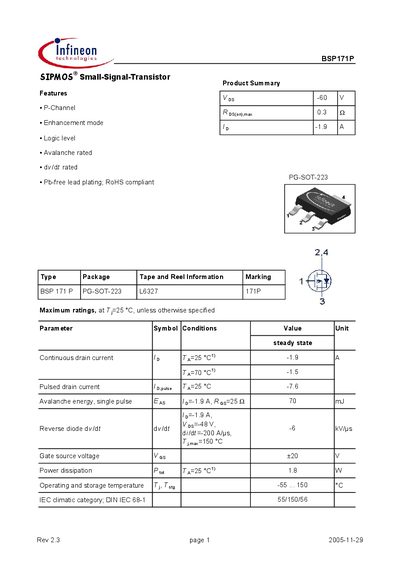
The BSP171P is a small‑signal P‑channel MOSFET offered in a PG‑SOT‑223 package. The document lists its key features such as low on‑resistance, enhancement‑mode operation, avalanche and dv/dt ratings, and compliance with RoHS.
Detailed specifications include maximum continuous and pulsed drain currents, breakdown voltage, thermal characteristics, dynamic switching parameters, and the recommended PCB footprint. Package dimensions and tape‑and‑reel handling information are also provided.
| Continuous drain current (Id) | -1.9 A |
|---|---|
| Pulsed drain current (Id,pulse) | -7.6 A |
| Drain‑source breakdown voltage (Vds) | -60 V |
| Gate‑source threshold voltage (Vgs(th)) | -2 V |
| On‑state resistance (Rds(on)) | 0.3 Ω |
| Power dissipation (Pd) | 18 W |
| Operating temperature range | -55 °C to 150 °C |
The BSP171P can conduct a continuous drain current of –1.9 A at 25 °C.
The device is supplied in a PG‑SOT‑223 (SOT‑223) package.
The maximum power dissipation is 18 W at a case temperature of 25 °C.
The breakdown voltage is specified as –60 V.