
BSP295 is a SIPMOS Small-Signal-Transistor with the features of N-Channel, Enhancement mode, dv/dt rated, PG-SOT-223 package.
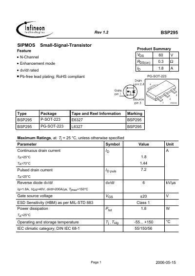
The BSP295 is an N‑channel, enhancement‑mode small‑signal transistor offered by Infineon Technologies. It is supplied in a PG‑SOT‑223 (SIPMOS) package and is RoHS compliant. The document provides detailed electrical, thermal, and dynamic characteristics for design engineers.
Key parameters include a maximum drain‑source voltage of 60 V, continuous drain current of 1.8 A, typical on‑resistance of 0.22 Ω, and gate‑threshold voltage around 0.8 V. Thermal resistance, capacitances, and switching times are also listed for accurate modeling in circuits.
| Maximum Drain‑Source Voltage (VDS) | 60 V |
|---|---|
| On‑Resistance (RDS(on)) typical | 0.22 Ω |
| Gate Threshold Voltage (VGS(th)) typical | 0.8 V |
| Output Capacitance (Coss) | 95 pF |
| Reverse Transfer Capacitance (Crss) | 45 pF |
| Package Type | PG‑SOT‑223 |
The BSP295 can withstand up to 60 V between drain and source.
The transistor is supplied in a PG‑SOT‑223 (SIPMOS) package.
Typical RDS(on) is about 0.22 Ω at VGS = 10 V and ID = 1.8 A.