
BSP129 is an N-channel, depletion mode, dv/dt rated small signal transistor available with a VGS(th) indicator on reel. It complies with RoHS and features lead-free lead plating.
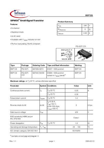
This document presents the technical data for the Infineon BSP129 small‑signal N‑channel MOSFET, including its electrical, thermal, and dynamic characteristics. It also lists package information, ordering codes, and safety notices.
Key sections cover product summary, maximum ratings, thermal and electrical parameters, dynamic behavior, gate‑charge data, and package outline, allowing designers to assess suitability for their circuits.
| Continuous drain current (Id) typ @ 25 °C | 0.35 A |
|---|---|
| Pulsed drain current (Id,pulse) @ 20 °C | 1.4 A |
| On‑state resistance (Rds(on)) max | 6 mΩ |
| Thermal resistance (junction‑to‑solder) | 25 K/W |
The BSP129 is supplied in a PG‑SOT‑223 package.
The device is rated for a continuous drain current of 0.35 A, pulsed drain current of 1.4 A, drain‑source breakdown voltage of 240 V, Rds(on) up to 6 mΩ, and operates from –55 °C to 150 °C.
The thermal resistance (junction‑to‑solder) is 25 K/W.