
This document describes the features and characteristics of the SPD06N60C3 CoolMOSTM power transistor, including new revolutionary high voltage technology, ultra low gate charge, periodic avalanche rated, high peak current capability, ultra low effective capacitances, extreme dv/dt rated, and improved transconductance.
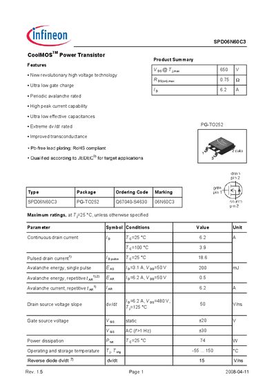
The SPDO6N60C3 is a CoolMOS power transistor featuring a high voltage rating of 600 V, low on‑state resistance, and ultra‑low gate charge. It is RoHS compliant and qualified according to JEDEC standards for target applications.
The document provides maximum ratings, thermal characteristics, electrical and dynamic parameters, as well as typical characteristic curves and safe operating area information for design engineers.
| Continuous drain current (Id) | 6.2 A |
|---|---|
| Pulsed drain current (Ipp) | 18.6 A |
| Drain‑source breakdown voltage (Vds) | 600 V |
| On‑state resistance (Rds(on)) | 0.75 Ω max |
| Gate charge (Qg) | 3.3 nC |
| Input capacitance (Ciss) | 620 pF |
| Output capacitance (Coss) | 200 pF |
| Power dissipation (Pd) at 25 °C | 74 W |
| Operating temperature range | -55 °C to 150 °C |
The maximum continuous drain current is 6.2 A at 25 °C.
The device is rated for a drain‑source breakdown voltage of 600 V.
The typical gate‑to‑source charge is 3.3 nC.
Yes, the device is Pb‑free and RoHS compliant.