
The SPP1413 is a P-Channel enhancement mode power MOSFET produced using high cell density DMOS trench technology. It is particularly suitable for low voltage applications such as power management in cellular phones and notebook computers, as well as other battery-powered circuits requiring high-side switching and low power loss. It features a super high density cell design for extremely low on-resistance and maximum DC current capability. The package is SOT-323 (SC-70).
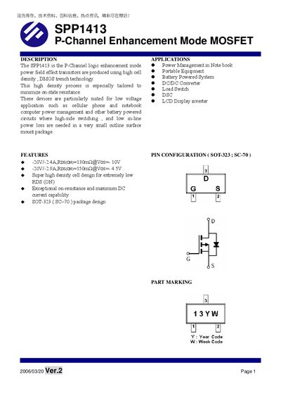
The SPP1413 is a P‑Channel logic enhancement mode MOSFET designed for low‑voltage power management in notebook, cellular phone, and other battery‑powered circuits. Its high‑density DMOS trench technology enables low on‑state resistance and high current capability in a compact SOT‑323 (SC‑70) package.
Key features include a maximum drain‑source voltage of –20 V, typical on‑resistance as low as 0.30 Ω, and a wide range of operating temperatures. The datasheet lists pin configuration, ordering information, absolute maximum ratings, electrical characteristics, and typical performance curves.
| Drain‑Source Voltage (V_DSS) | -20 V |
|---|---|
| Gate‑Source Voltage (V_GS) | +12 V |
| Continuous Drain Current (ID) at 70 °C | -2.0 A |
| Pulsed Drain Current (I_pM) | 8 A |
| Package Type | SOT‑323 (SC‑70) |
The maximum drain‑source voltage is –20 V.
It is supplied in a SOT‑323 (SC‑70) surface‑mount package.
The gate threshold voltage ranges from –0.5 V to –1.8 V.
The device can handle a continuous drain current of –2.0 A at 70 °C.