
SPP3401B is the P-Channel logic enhancement mode power field effect transistors are produced using high cell density , DMOS trench technology. This high density process is especially tailored to minimize on-state resistance. These devices are particularly suited for low voltage application such as cellular phone and notebook computer power management and other battery powered circuits, and low in-line power loss are needed in a very small outline surface mount package.
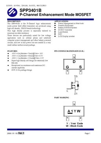
The SPP3401B is a P‑Channel logic‑level enhancement MOSFET designed for low‑voltage, battery‑powered applications such as cellular phones and notebook computers. It features a high‑density DMOS trench structure that minimizes on‑state resistance and supports high current capability in a compact SOT‑23‑3L package.
The datasheet lists absolute maximum ratings, typical electrical characteristics, and package dimensions. Key parameters include a -30 V drain‑source voltage, +12 V gate‑source rating, low on‑resistance (≈0.08 Ω), and a total gate charge of about 10 nC. Package outline dimensions and ordering information are also provided.
| Drain‑Source Voltage (V_DSS) | -30 V |
|---|---|
| Gate‑Source Voltage (V_GSS) | +12 V |
| Continuous Drain Current (Ta=25 °C) | -4.0 A |
| On‑Resistance (R_DS(on)) | 0.080 Ω (V_GS=-4.5 V, I_D=-3.2 A) |
| Total Gate Charge (Q_g) | 10 nC |
| Package | SOT‑23‑3L |
The device is rated for a maximum drain‑source voltage of -30 V.
Typical on‑resistance is about 0.080 Ω at V_GS = -4.5 V and I_D = -3.2 A.
The MOSFET is supplied in a SOT‑23‑3L surface‑mount package.
Yes, it is designed for low‑voltage applications such as cellular phones and notebook computers.